ysl-cnc semiconductor-parts

What are the special requirements for CNC machining of semiconductor equipment parts?

The special requirements for CNC machining of semiconductor equipment parts focus on four areas: materials must meet the cleanliness and corrosion-resistance conditions of the process environment; surface roughness and geometric tolerances directly affect the performance of chambers and gas lines; parts must undergo traceable cleaning and cleanroom packaging before shipment; and the tolerance and inspection records for each batch must be verifiable by the buyer. These four requirements are interconnected, and missing any one of them can cause the part to fail in the front-end process.

Key Takeaways

  • Cleanliness and Corrosion Resistance Are Core to Material Selection

    Semiconductor component materials must meet process environment cleanliness and corrosion resistance requirements. Aluminum alloys, stainless steel, brass, etc., are selected based on the process stage, not just by cutting according to the drawing.

  • Surface Roughness Is a Functional Indicator

    Rough surfaces absorb moisture and organics, which outgas in vacuum environments and affect gas flow. Internal surfaces often require Ra below 0.8 μm, with stricter requirements for sealing surfaces.

  • Cleaning and Dust-Free Packaging Are Shipping Prerequisites

    Before shipment, parts must undergo ultrasonic cleaning, deionized water rinsing, and drying, then be double-bagged in dust-free bags in a low-particle environment. The cleaning level and packaging method must be clearly documented.

  • Inspection Records Must Be Traceable for Re-Verification

    Measurement data, gauge numbers, and operator information for each batch should be recorded, allowing buyers to perform incoming re-inspection and process traceability, rather than just providing pass/fail results.

What is the difference between semiconductor equipment parts and general precision metal parts?

General precision metal parts can be delivered as long as dimensional tolerances and appearance meet the drawing, but semiconductor equipment parts must pass two additional checks: compatibility with the process environment and cleanliness. The former means that parts must not outgas, corrode, or contaminate the chamber in vacuum, etching gas, or high-purity chemical environments; the latter means that particles, oils, and residues on the part surface at the time of delivery must be below the buyer's specification. These two requirements feed back into material selection, tooling strategy, cutting fluid, and packaging methods, so the CNC machining of semiconductor parts cannot directly apply the production process used for general precision parts. Before placing an order, buyers should confirm that the supplier understands this difference, rather than only looking at the machine grade.

Six capabilities buyers most often check when machining semiconductor equipment parts

  • Material selection matched to the process environment

    Aluminum alloys, stainless steel, brass, and other materials have different suitability for different process stages. Buyers should confirm that the supplier can recommend materials based on chamber or line application, rather than simply cutting to the drawing.

  • Achievable surface roughness at the Ra level

    The internal surfaces of vacuum chambers and gas lines often require Ra 0.8 μm or finer. The machining strategy and tool condition must be matched to this level.

  • Stable geometric tolerances and roundness

    The profile and position tolerances of O-ring grooves, sealing surfaces, and flange mating faces directly affect the chamber leak rate and must be verified with a coordinate measuring machine.

  • In-process and pre-shipment inspection procedures

    A three-stage process of incoming inspection, in-process sampling, and final pre-shipment inspection is the basic threshold for traceability of semiconductor parts.

  • Pre-shipment cleaning and cleanroom packaging

    Cleaning level, packaging environment, and packaging materials all affect cleanliness. Buyers should require the supplier to state which cleaning solution and packaging method are used.

  • Traceable inspection records and measurement reports

    The measurement data, gauge numbers, and operators for each batch of parts should be traceable to facilitate the buyer's incoming re-inspection and process traceability.

How should materials and surface specifications for semiconductor parts be selected?

Material selection for semiconductor equipment parts is not based solely on strength but on the process stage. Common aluminum alloys are often used for chamber housings and brackets because they are lightweight and dissipate heat quickly; stainless steel is often used inside vacuum chambers and for gas lines, where corrosion resistance and low outgassing are the main considerations; brass and copper are found in parts requiring electrical or thermal conductivity, but note that copper-based materials are not suitable in certain etching environments. For surface specifications, internal surfaces in contact with process gases typically require Ra 0.8 μm or finer, while sealing surfaces require stricter profile tolerances. When requesting a quote, buyers should proactively provide the process stage and contact media information so the supplier can recommend material grades and surface treatments accordingly, rather than only providing a 2D drawing.

semiconductor parts scene 1

Why Are Semiconductor Parts Particularly Sensitive to Surface Roughness?

Surface roughness in semiconductor equipment is not merely a cosmetic indicator but a functional one. A rough surface increases surface area, which can adsorb more moisture and organic contaminants, slowly outgassing in a vacuum environment and affecting the time required for the chamber to reach the target vacuum level. Rough inner walls of tubing can also cause process gases to form turbulence or stagnant zones, leading to uneven etching or deposition. For sealing surfaces, roughness directly determines whether an O-ring or metal seal can achieve the required leak rate. Therefore, surface roughness requirements for semiconductor parts are often one to two grades stricter than for general mechanical parts. Machining requires sharp tools, stable cutting parameters, and, when necessary, a secondary finishing operation. Buyers should clearly specify the Ra value and measurement locations on the drawing to prevent suppliers from delivering to general precision part standards.
What Are the Machining and Cleaning Requirements for Vacuum Chamber Parts?

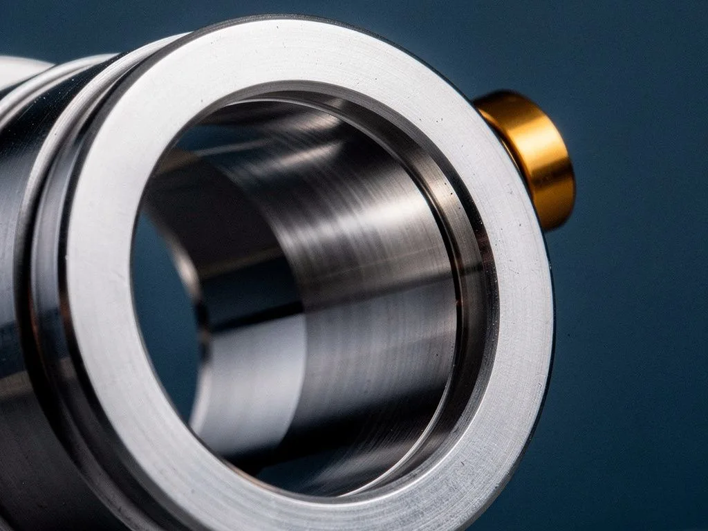
The key to machining vacuum chamber parts lies in maintaining sealing integrity and internal cleanliness. Machined surfaces should avoid sharp corners and edges, as these areas tend to retain cutting fluid and particles. All surfaces that come into contact with vacuum should avoid markers or coatings that may outgas. Special attention must be paid to tool accessibility and chip evacuation in threaded holes, blind holes, and recessed areas. For cleaning, parts should undergo ultrasonic cleaning, deionized water rinsing, and drying after machining. Depending on buyer specifications, nitrogen purging or vacuum baking may also be required. Packaging must be performed in a low-particle environment, using cleanroom bags and double-layer packaging. When evaluating suppliers, buyers should actually visit the facility or request photos to confirm the environmental classification of the cleaning and packaging areas, rather than relying solely on documented procedures.

Semiconductor Parts Inspection Process

  1. 1

    Incoming Material Inspection

    Verify that materials meet process environment requirements, checking material grades and suitability for chamber or tubing applications.

  2. 2

    In-Process Sampling

    Sample key dimensions and surface roughness during machining to ensure tool condition and cutting parameters remain stable.

  3. 3

    Final Inspection Before Shipment

    Verify geometric tolerances using CMM, profilometers, and roughness testers, and record measurement data and gauge numbers.

  4. 4

    Cleaning and Dust-Free Packaging

    After ultrasonic cleaning, deionized water rinsing, and drying, package in double dust-free bags in a low-particle environment for shipment.

semiconductor parts scene 2

How Are Tolerances for Semiconductor Parts Verified and Documented?

Tolerance verification for semiconductor parts cannot rely solely on first-article or last-article inspection; a traceable measurement system must be established. Common practice involves using coordinate measuring machines, profilometers, and surface roughness testers to perform full or sampling inspection on critical dimensions, recording measurement data along with the gauge number, operator, and date. For critical geometries such as sealing surfaces, O-ring grooves, and flange mating faces, it is recommended to specify roundness, parallelism, and position tolerance on the drawing and require the supplier to provide corresponding measurement reports. When auditing suppliers, buyers should confirm the calibration status of their measurement equipment and the measurement uncertainty, as these two factors directly affect the credibility of the data. If a supplier only provides a binary "pass/fail" result without continuous measurement data, it will be difficult for the buyer to perform process traceability and anomaly analysis.

What Capabilities Are Needed to Move from General Mechanical Parts into the Semiconductor Supply Chain?

A machining shop that originally handled general mechanical parts must develop at least three types of capabilities to enter the semiconductor equipment supply chain. The first is material and process knowledge: it must understand the material restrictions of different process stages, such as which alloys cannot be used in chlorine-containing environments and which surface treatments may outgas. The second is cleanliness control: including the classification of the machining environment, selection of cutting fluids, cleaning procedures, and packaging methods, which are rarely strictly required in general machining. The third is a quality documentation system: semiconductor buyers often require PPAP, measurement reports, material certificates, and traceability records, and the document formats differ from those for general mechanical parts. After developing these three capabilities, a more practical entry path is to gradually verify process stability through trial parts. When evaluating new suppliers, buyers also assess these three aspects rather than deciding solely on price or lead time.

FAQ

What distinguishes semiconductor equipment parts from general precision metal parts?

Beyond dimensional tolerances and appearance, semiconductor equipment parts must pass process environment compatibility and cleanliness requirements. Parts must not outgas, corrode, or contaminate the chamber in vacuum, etching gas, or high-purity chemical environments. Surface particles, oils, and residues must be below buyer specifications at shipment, so production processes cannot directly follow those for general precision parts.

Why are semiconductor parts so sensitive to surface roughness?

Surface roughness is a functional indicator, not just an appearance one. Rough surfaces increase surface area, adsorb more moisture and organic contaminants, and slowly outgas in vacuum, affecting the time to reach target vacuum levels. Rough internal surfaces in tubing can also cause turbulence or stagnant zones in process gases, leading to uneven etching or deposition. Sealing surface roughness directly determines leak rates.

What are the machining and cleaning requirements for vacuum chamber parts?

Machined surfaces should avoid sharp corners and edges to prevent coolant and particle accumulation. Surfaces in contact with vacuum should avoid markers or coatings that outgas. After machining, parts should undergo ultrasonic cleaning, deionized water rinsing, and drying. Depending on specifications, nitrogen purging or vacuum baking may be required. Packaging must be double-bagged in dust-free bags in a low-particle environment.

How are tolerances for semiconductor parts verified and recorded?

Tolerance verification cannot rely only on first or last articles; a traceable measurement system must be established. Common tools include CMM, profilometers, and surface roughness testers. Key dimensions are fully or sample inspected, with measurement data, gauge numbers, operator, and date recorded. Sealing surfaces, O-ring grooves, and flange mating faces should have roundness, parallelism, and position tolerance indicated, and suppliers should provide measurement reports.

What capabilities are needed to move from general machining into the semiconductor supply chain?

At least three capability areas are needed: material and process knowledge to understand material restrictions across process stages; cleanliness control including machining environment classification, coolant selection, cleaning procedures, and packaging methods; and a quality documentation system, as semiconductor buyers often require PPAP, measurement reports, material certificates, and traceability records. After building these, process stability should be validated through trial parts.

Looking for a CNC machining supplier for semiconductor parts?

If you are seeking a CNC machining partner capable of meeting semiconductor process environment requirements, please provide your part drawings, process stage, and cleanliness requirements. We will then evaluate whether the materials, machining strategy, and inspection procedures are suitable.